SK hynix HBM Packaging at Hot Chips 2026
ServeTheHome — sK hynix’s Hot Chips 2026 presentation is around high-bandwidth memory (HBM) and advanced packaging. From a slide flip, it looks like they will be covering the 3D stacking, bonding, and system integration choices behind high-bandwidth memory.
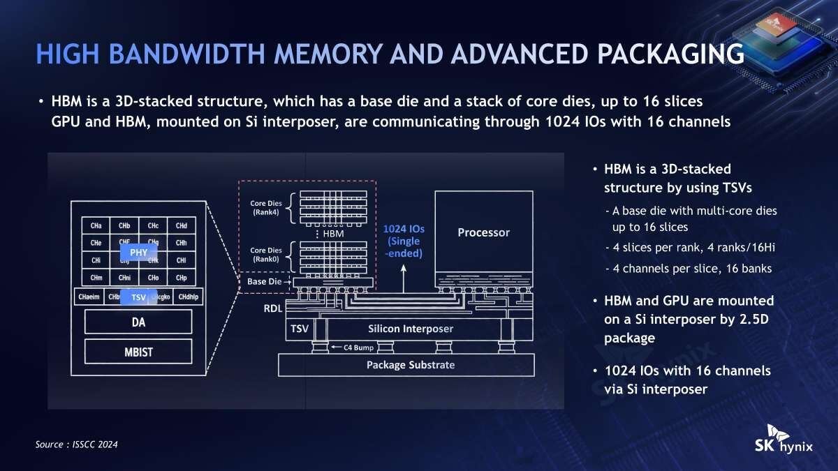
Like the others, we are doing these live, so please excuse typos. SK hynix began by explaining that HBM is a 3D-stacked structure comprising a base die and a stack of core dies, up to 16 slices in total. GPU and HBM sit together on a silicon interposer in a 2.5D package and communicate via 1024 IOs across 16 channels, with four slices per rank and four ranks in a 16-high stack. Getting that interposer connection right matters because it is where HBM meets the accelerator. Higher bandwidth, higher capacity, and higher power efficiency are the why behind advancing HBM. Despite the per-GB cost being higher for HBM, SK hynix argues that wider HBM adoption saves space, power, and operating costs. This is a bit of an interesting comparison, but it is showing 12x GDDR6 sites versus 4x HBM3E sites as being more space efficient while providing more bandwidth and capacity. This seems like a bit of an odd direct comparison point since cards like the consumer(-ish) NVIDIA GeForce RTX 5090 have 32GB of GDDR7, but OK. Capacity and bandwidth climb with every HBM generation. HBM2E delivered 460 GB/s, HBM3 moved to 717 GB/s, HBM3E reached 1024 GB/s, and HBM4 doubles the picture with 2048 GB/s across 2048 IOs. Package size grows too, from a 10×11 mm base to a 12.4×11 mm footprint on HBM4. HBM4 has more TSVs and micro-bumps. SK hynix lists over 20K TSVs and 16148 base micro-bumps on a 12.8×11 mm part with a 775 um Z-height, targeting more than 2 TB/s of bandwidth with a 40+ percent power-efficiency gain and improved thermal resistance. Capacity climbs to 48 GB, with 12-high in production and 16-high under qualification. Stacking die-to-die has two main bonding choices, and SK hynix lays out the trade-off between thermo-compression bonding with non-conductive film and mass reflow with molded underfill.