Samsung Evolving HBM Base Die at Hot Chips 2026
ServeTheHome — at Hot Chips 2026, Samsung is presenting Evolving HBM Base Die, a look at how the company wants to turn the base die of high-bandwidth memory into something far more capable than a passive interposer. We are covering this talk live, so please excuse any typos.
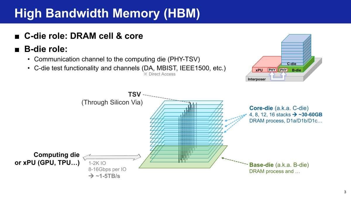
HBM splits its work between the DRAM core dies stacked above and the base die underneath. Samsung calls the stacked memory layers C-dies, while the base die, or B-die, carries the PHY and through-silicon vias that form the communication channel to the compute die. Four, eight, twelve, or sixteen C-die stacks land on that base die. If you need a visual, here is the diagram. HBM bandwidth and capacity have climbed steadily since the first generation. Samsung’s historical figures trace maximum capacity from roughly 1 GB and 1 TB/s in the original HBM through to an HBM5 generation that pushes past 60GB and 6 TB/s. Rising bandwidth, more than capacity alone, keeps forcing fundamental changes in the base die. Several limits throttle how fast HBM bandwidth can grow. Samsung points to through-silicon via counts and pitch on both the C-die stack and the base die, along with the I/O count and speed of the PHY embedded in the B-die. Here are TSV and DQ counts against pitch and area across generations to show where the pressure builds. Process technology for the C-die stays on DRAM-class nodes, but the base die has started to move. Samsung’s trend table shows the B-die shifting from older logic process toward 4nm starting with HBM4, narrowing the gap to the XPU SoC. Even as energy efficiency improves, MPGA power keeps rising, which is why Samsung says advanced logic in the B-die becomes essential from HBM4 onward. Samsung applied its D1c DRAM process and logic 4nm to HBM4, with power reduction as the primary goal. Active area minimization matters too, and this work marks the beginning of true DRAM and advanced logic integration.